
Pin Header Mating Length, Tail Length and Stack Height: Check the Complete Chain
Table of Contents
A request for a “longer pin header” leaves the critical dimension unresolved. The extra length could be required above the insulator for mating, below it for PCB termination, or between the two boards. Changing one dimension does not necessarily satisfy the other two.
Define the post, the socket's permitted insertion, both PCB thicknesses and the finished board spacing as one dimension chain. This guide works through a documented original-component pair using a fictional nominal installation. It does not prescribe a universal stack height or approve a replacement by appearance.
Build the board-spacing chain from named dimensions
Nominal illustrative geometry for TSW-105-07-L-D and SSW-105-01-L-D. The assumed 12.00 mm board gap is not a recommended stack height.
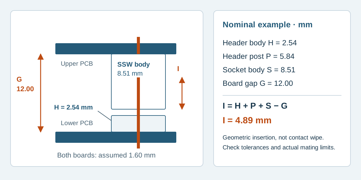
Conceptual illustration. Fictional examples are not approved product configurations, tooling instructions or inspection results.
Name the datums before adding lengths
For a parallel board-to-board arrangement, call the facing PCB surfaces the lower-board inner surface and upper-board inner surface. Let G be their separation. The header is seated on the lower inner surface; the socket is seated on the upper inner surface and faces downward toward it.
Scroll sideways to read all columns.
| Symbol | Definition for this example |
|---|---|
| H | Header insulator height above its PCB seating surface |
| P | Header post length from insulator top to pin tip |
| S | Socket height from its PCB seating surface to its mating entry face |
| I | Pin insertion from the socket entry face to the pin tip, along the mating axis |
| G | Separation between the two facing PCB seating surfaces |
| T1 / T2 | Lower and upper PCB thicknesses |
| L1 / L2 | Tail lengths measured from each connector's PCB seating surface |
These definitions concern geometry. I is not the length over which the socket spring touches the pin, and it is not contact wipe. The socket's contact location and required engagement must come from the applicable manufacturer documentation. Visible exposed pin length cannot identify that hidden contact relationship.
The through-hole versus SMT guide addresses attachment methods. Here, both parts use through-hole tails so the dimensional relationship can be followed consistently.
Start with a documented header and socket pair
Samtec lists SSW-105-01-L-D as a mating part for TSW-105-07-L-D on the header's official page. Both are ten-contact, double-row examples. Preserve the complete references; another lead style changes the geometry.
The TSW catalog, straight-pin style -07 and SSW through-hole catalog provide the following dimensions. Values are shown in the manufacturer's metric presentation for the nominal example.
Scroll sideways to read all columns.
| Dimension | Value used | Reference |
|---|---|---|
| TSW post P | 5.84 mm | Style -07, dimension C |
| TSW tail L1 | 2.54 mm | Style -07, dimension B |
| TSW insulator H | 2.54 mm | Straight-pin geometry; 10.92 − 5.84 − 2.54 mm |
| SSW socket S | 8.51 mm | Straight-pin socket body height |
| SSW tail L2 | 2.64 mm | Standard insertion-force style -01, dimension A |
| SSW insertion range | 3.68 to 6.35 mm | Catalog insertion-depth specification |
These fields are enough to check a nominal proposal, not a complete tolerance release. Manufacturer inch dimensions, individual tolerances, seating conditions and relevant notes still control the real design.
Work through a fictional 12 mm installation
Suppose an equipment drawing EX-STACK-03 proposes G = 12.00 mm between the two facing PCB seating surfaces. This is an illustrative design input, not a Samtec recommended stack height. Assume both connectors are seated as defined, boards are parallel and there is no additional mounting offset.
The pin tip's height above the lower PCB is H + P. The socket entry lies at G − S above that same reference. Therefore:
I = H + P + S − G = 2.54 + 5.84 + 8.51 − 12.00 = 4.89 mm.
The nominal insertion lies inside the quoted catalog range. It also stays within the available 5.84 mm post. The housing-to-housing space is G − H − S = 0.95 mm. Those are geometric observations under the stated assumptions, not proof that every tolerance combination assembles correctly.
Now assume each PCB is 1.60 mm thick. The nominal unsoldered tail projection beyond the opposite PCB surface is:
Scroll sideways to read all columns.
| Side | Calculation | Nominal projection |
|---|---|---|
| Lower header | L1 − T1 = 2.54 − 1.60 mm | 0.94 mm |
| Upper socket | L2 − T2 = 2.64 − 1.60 mm | 1.04 mm |
These projections are not solder-joint acceptance limits. The PCB assembler must assess actual hole design, board stack-up, solder process and inspection requirements. Solder volume and the final joint envelope are not included in this simple subtraction.
Check both ends of the tolerance chain
A nominal calculation can pass while real parts under-engage or collide. For the defined equation, increasing G decreases insertion; increasing H, P or S increases it. Evaluate the minimum and maximum insertion using the actual controlled dimensions and installation conditions, rather than assigning an arbitrary tolerance to every field.
At the low-insertion extreme, check adequate engagement against the manufacturer's requirement. At the high-insertion extreme, check permitted insertion and physical interference, including the finite post, housing positions and anything beyond the socket entry. Do not force housings together to obtain a preferred board spacing.
Add board flatness, relative angular alignment, seating variation and mechanical support as applicable. If a standoff fixes the board separation, its length and mounting faces are part of the chain. Samtec recommends board-to-board support hardware in its SSW/TSW specification, section 4.8; the connector need not be treated as the assembly's only structural support.
Keep the drawing and sourcing request consistent
State whether stack height means facing board surfaces, outside board surfaces or another datum. In the fictional example, outside-to-outside spacing would also include both PCB thicknesses; it is a different dimension from G.
List both connector references and their orientation, mounting faces, board thicknesses, spacing requirement and tolerances. Mark the required post and tail dimensions separately if the component configuration remains open. A longer tail cannot correct inadequate socket insertion, and a longer post cannot create underside solder clearance.
A proposed compatible alternative needs its own mating and dimension evidence. A successful hand fit or the same nominal pitch does not transfer the original pair's engagement requirements or qualification results.
Stack-height questions
Is the exposed post the mating contact length?
No. It is a geometric length from a defined insulator surface to the tip. Insertion and the actual spring-contact engagement are separate quantities.
Can I calculate spacing by adding the two body heights?
That only describes a particular housing relationship. Use the permitted insertion and any required body clearance to establish the installed spacing; do not assume touching housings is the intended condition.
Does a longer solder tail permit a higher board stack?
A tail serves the PCB termination side in this example. Stack height depends on the mating-side geometry and installed datums; changing the tail alone does not extend the post.
Send the complete dimension chain for review
For custom pin headers or female headers, send the exact pair references, both PCB thicknesses, required spacing datum and tolerances. Include the enclosure and support arrangement when they constrain the stack. Zeakka coordinates sourcing and supplier clarification as a trading partner; this reference example does not offer loose original Samtec components or establish an interchangeable alternative. Contact Zeakka with the drawing and identify which dimensions are fixed.
Share this article
Help others discover this content