
Single-Row vs Dual-Row Headers: Compare the Installed Layout at Equal Circuit Count
Table of Contents
At the same circuit count, a dual-row header can shorten the contact field while making it wider. That geometric change affects routing, connector access and the board area available around the interface. It does not make one arrangement automatically better or electrically equivalent to the other.
Compare installed alternatives with the same ten required circuits, their specified mates and an explicit contact assignment. A smaller rectangle on the PCB is useful only when the board can route it, the equipment can assemble it and the resulting connection matches the intended circuit map.
Compare ten circuits by center span and row spacing
Based on the nominal pitch of the cited Samtec TSW layouts. Dots are unnumbered so the drawing cannot be mistaken for a universal pin-number convention.
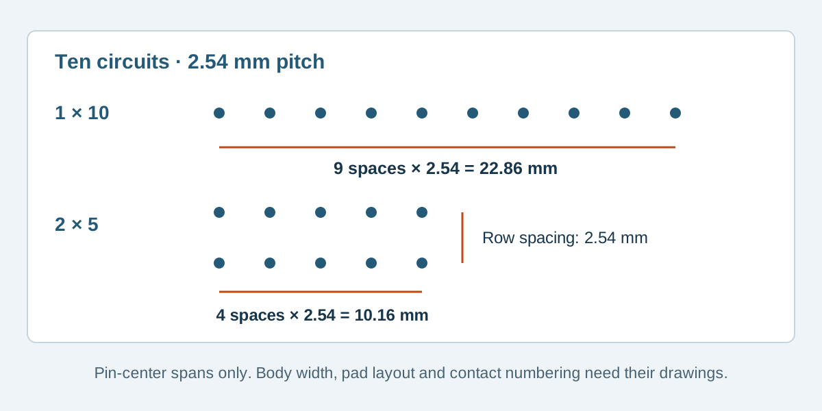
Conceptual illustration. Fictional examples are not approved product configurations, tooling instructions or inspection results.
Hold the circuit count constant
Two original Samtec examples provide a checkable reference: TSW-110-07-L-S has one row of ten contacts, while TSW-105-07-L-D has two rows of five. Both use a 2.54 mm position pitch and lead style -07.
Their official pages identify SSW-110-01-L-S as a mate for the single-row example and SSW-105-01-L-D for the dual-row example. These are documentation examples, not a claim that a socket can be moved unchanged between the two layouts.
The relevant header drawing is TSW-XXX-XX-XXX-X-XX-XXX, revision DS. Its companion recommended PCB layout is the TSW-XXX-XX-X-X-XX-XXX footprint, revision A. Consult the selected configurations, not a generic photograph of the series.
Separate center span, header body and mating body
For n contacts along one row at pitch p, the first-to-last contact-center span is (n − 1) × p. It is shorter than the complete housing. In the dual-row example, the second direction adds a separate row spacing.
Scroll sideways to read all columns.
| Nominal geometry | Single row: 1 × 10 | Dual row: 2 × 5 |
|---|---|---|
| Along-row contact pitch | 2.54 mm | 2.54 mm |
| First-to-last center span along a row | 9 × 2.54 = 22.86 mm | 4 × 2.54 = 10.16 mm |
| Row-center spacing | Not applicable | 2.54 mm |
| TSW header body length | 25.40 mm | 12.70 mm |
| TSW header body width | 2.54 mm | 5.08 mm |
| SSW mate body length | 25.91 mm | 13.21 mm |
| SSW mate body width | 2.41 mm | 4.95 mm |
The header's center-spacing basis is in the recommended PCB layout. Body dimensions are from the TSW straight-pin catalog and SSW through-hole catalog. Values summarize the indicated nominal/reference geometry and omit manufacturing tolerances.
The dual-row contact field is shorter, but its body is wider. The mating socket also extends beyond the header's nominal length in these examples. A board-edge clearance based only on pin centers can therefore miss part of the installed connector. Add solder joints, board features and handling space to the design review; this table is not a complete keep-out definition.
Route the same ten nets through both candidates
Use a real PCB routing review rather than assuming that two rows halve the required board space. A long single row can distribute circuits along an edge. A compact dual row brings more connections into a shorter span and may make the routes between pads and nearby components more constrained.
The result depends on pad dimensions, routing rules, layers, neighboring copper and the net assignment. Do not promise that either alternative routes on a particular layer count without checking that design. Likewise, shorter connector length does not independently establish better signal performance or power handling.
For a fictional circuit set EX-LAYOUT-03, preserve net identity in a mapping table before relocating the interface:
Scroll sideways to read all columns.
| Equipment net | Single-row contact ID | Dual-row contact ID |
|---|---|---|
| N01 | 1 | 1 |
| N02 | 2 | 2 |
| N03 | 3 | 3 |
| N04 | 4 | 4 |
| N05 | 5 | 5 |
| N06 | 6 | 6 |
| N07 | 7 | 7 |
| N08 | 8 | 8 |
| N09 | 9 | 9 |
| N10 | 10 | 10 |
This is an illustrative assignment, not a standard pinout. The columns list contact identifiers; they are not mating-face views and do not say that a physical row contains contacts 1 through 5. Net names here carry no implied power, ground or signal function.
The TSW drawing, sheet 3, figure 3 shows numbering for its row arrangements. Carry the correct identifiers into the PCB symbol, footprint and mating-part map. Do not reuse a generic numbering pattern or mirror the socket view mentally. The pinout and viewing guide explains that separate viewpoint check.
Review placement and removal with both boards present
A dual-row part may save length while putting its gripping surfaces close to nearby components. A single-row part may leave a long, narrow interface that needs a different handling motion. Check where the operator grips the mate and where assembly and removal forces enter the PCB.
For a board-to-board pair, consider board support, alignment and how multiple connectors engage together. For a cable interface, add the actual cable-side mate and exit route rather than reusing the board-socket envelope from this example. A permitted mate family still needs its exact configured drawing.
Do not assign a universal insertion-force advantage from row count. Contact design, populated positions, finishes, alignment and the complete mating arrangement matter. If force or accessibility constrains the product, specify the required conditions for review rather than relying on a broad “easy to plug in” description.
The mating-length and stack-height guide addresses the vertical dimension chain. The present comparison changes the plan layout and contact arrangement; height remains a separate requirement.
Treat a row-count change as an interface revision
Changing from one row to two requires corresponding work on the mate and its circuit assignment. Review the schematic symbol, PCB footprint, mechanical drawing, BOM and any cable test reference together. An unchanged net name does not prevent an incorrect footprint pin assignment.
For an existing product, identify which items can change. If the mating cable or daughterboard must remain, that constraint may rule out an otherwise attractive footprint. If the interface is being redesigned, document both approved halves and the revision transition before ordering samples.
The connector component guide helps distinguish headers, housings and contacts. It does not replace the exact drawing needed for this layout decision.
Row-layout questions
Is a two-by-five header half the size of a one-by-ten?
It has fewer pitch intervals along a row, but it adds width and has its own housing and mate. Compare the full outline and access requirements, not only the contact count.
Do dual-row contacts always number across the rows?
No universal convention should be assumed. Use the selected manufacturer's drawing and its defined view, then verify the PCB and mating-part identifiers against it.
Can I keep the old cable after changing row count?
Only if the complete interface remains compatible, which a row-count change generally requires reviewing explicitly. Confirm the actual mate and every circuit connection before approving the revision.
Request a layout comparison with the actual mating pair
For custom pin headers and female headers, send the two candidate part references, required circuits, board area, spacing and intended mate. Include the current pin map and identify fixed equipment constraints. Zeakka coordinates sourcing and supplier clarification as a trading partner. These original-component examples do not offer loose original parts or qualify alternatives. Send the layout for review before treating a row-count change as an interchangeable purchasing option.
Share this article
Help others discover this content